PCB design softwares: Difference between revisions
From wikiluntti
| (7 intermediate revisions by the same user not shown) | |||
| Line 17: | Line 17: | ||
# editing symbols: Symbol Editor | # editing symbols: Symbol Editor | ||
# editing footprints: Footprint Editor | # editing footprints: Footprint Editor | ||
1. Schematics. Connect through | |||
# lines. (Gets complicated.) | |||
# network labels. | |||
# hierarchical labels. (Multiple worksheets.) | |||
# global labels. | |||
=== Arduino Uno custom shield === | === Arduino Uno custom shield === | ||
| Line 25: | Line 31: | ||
Kicad arduinoUno Schematic3.png| Copy the labels and the text and rectangle | Kicad arduinoUno Schematic3.png| Copy the labels and the text and rectangle | ||
Kicad arduinoUno Schematic4.png| Cut the wires from the unused connectors. | Kicad arduinoUno Schematic4.png| Cut the wires from the unused connectors. | ||
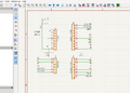
Kicad arduinoUno Schematic5.png| Some of the sensors are already in the kiCAD library. SO it is easy to include into the system. | |||
Kicad arduinoUno Schematic6.png| Cut the extra wires, save, and check the PCB Editor. Update PCB from schematics (Tools menu). Some components are missing | |||
Kicad arduinoUno Schematic7.png| Assign footprints. This is for a resistor. | |||
Kicad arduinoUno Schematic8.png| The footprints are assigned and all components are visible. | |||
Kicad arduinoUno Schematic9.png| The 3d view when the R1 is changed to axial. The yellow lines are routed in PCB view. | |||
</gallery> | </gallery> | ||
File → New Project From Template → Arduino Uno | File → New Project From Template → Arduino Uno | ||
References | |||
* https://www.youtube.com/watch?v=B6VE6SSA2wk | |||
* https://www.youtube.com/watch?v=ou_qRzNHZrw | |||
* https://www.youtube.com/watch?v=XRazkC7tdxo | |||
=== ESP32 + sensors === | === ESP32 + sensors === | ||
Latest revision as of 09:58, 14 February 2026
Introduction
- LibrePCB
- kiCAD
Kicad Tutorial
1
Workflow (a project-based workflow)
- drawing a schematic: Schematic Editor. Which components are in the design and how they are connected.
- custom symbols may need to be created if appropriate symbols aren't available.
- footprints are also selected for each component
- laying out a circuit board: PCB Editor
- footprints are the copper pads that match the pins on a physical component
- editing symbols: Symbol Editor
- editing footprints: Footprint Editor
1. Schematics. Connect through
- lines. (Gets complicated.)
- network labels.
- hierarchical labels. (Multiple worksheets.)
- global labels.
Arduino Uno custom shield
-
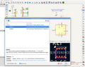
The connectors are already available at the Templates.
-
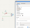
The values can be edited by E key.
-
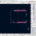
Copy the labels and the text and rectangle
-
Cut the wires from the unused connectors.
-
Some of the sensors are already in the kiCAD library. SO it is easy to include into the system.
-
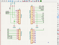
Cut the extra wires, save, and check the PCB Editor. Update PCB from schematics (Tools menu). Some components are missing
-
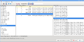
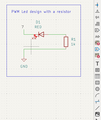
Assign footprints. This is for a resistor.
-
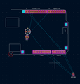
The footprints are assigned and all components are visible.
-
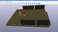
The 3d view when the R1 is changed to axial. The yellow lines are routed in PCB view.


File → New Project From Template → Arduino Uno
References
- https://www.youtube.com/watch?v=B6VE6SSA2wk
- https://www.youtube.com/watch?v=ou_qRzNHZrw
- https://www.youtube.com/watch?v=XRazkC7tdxo